The answer to ALL Your PCB needs
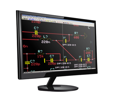
Draw hierarchical schematic diagrams with an unlimited number of pages. Local net definitions allow multiple instances of pages, enabling modular design flow.
Intelligent bus member enumeration speeds design entry and notation.
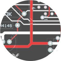
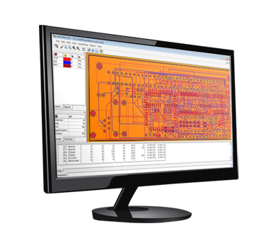
Powerful layout features include net guidelines, manual trace routing with optional mitering or Bezier curves, pin and group swap, automatic via generation, trace length and impedance calculators, global adjustment of annular ring size, connectivity and clearance rules check, intelligent copper pour and more.
Read more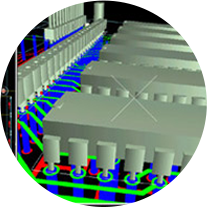
The CADint 3D Viewer allows you to view your board from any angle at nearly any magnification. Vertical clearance constraints for components can easy be visualized, as can any aspect of the PCB itself.
Custom 3D PCB Symbols and the completed designâs can be loaded directly into SolidWorks.
High quality, on time & at competitive prices
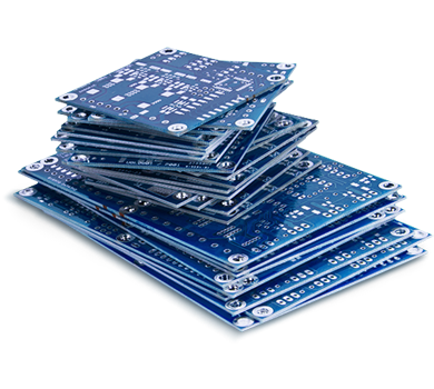
Creating one of the most advanced & powerful PCB CAD/CAM packages on the market today has also given us an incredible advantage in becoming one of the leading PCB suppliers on the Scandinavian market.
With over 35 years of PCB experience, your PCB production is safe in our hands.Read more