Schematic capture

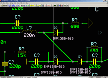
Take advantage of the nearly unlimited power of CADint schematic capture. Work with flat or hierarchical designs with an unlimited number of pages of any size. Signals may be defined as local to a page, common to a page and its parent or global. Pages may be easily copied to generate repeated modules in a design. Transfer critical information, such as component placement requirements or signal routing constraints to PCB as component or net properties.

Schematic capture features

  • Free or orthogonal wire and bus routing with automated junction generation
  • Automated bus member annotation
  • 39 drawing layers including 3 symbol drawing layers, 9 object annotation layers, 16 net-related layers and 11 documentation layers
  • Support for alphanumeric pin names.
  • Autopackaging and pin assignment.
  • Design rule checking (fanout, no driver or multiple drivers in net..)
  • Unlimited number of components, nets, nodes, etc. (unless limited by license)

Interfaces

  • Import schematic designs from CadStar, EDwin, EE Designer, Innoveda, P-Cad, and more.
  • Import graphics in DXF or Gerber format.

Libraries

  • Schematic symbol library with 1500 symbols representing more than 10,000 components
  • Flexible library structure supports generalized component types as well as specific part numbers
  • Powerful library browser with preview, import, export, etc.
  • Graphical symbol and library editors

System features

  • Versatile graphics primitives, including: line, arc, rectangle, circle, text, polygon line and arc with definable thickness filled circle filled rectangle with definable corner radius
  • Display objects as centerline, outline or filled; in solid or transparent colors
  • Powerful properties/attributes handling
  • Rotate, copy, move, and/or mirror any group of objects
  • Automatic rubber-banding of wires, etc during move, stretch and/or rotate
  • 0.1 micron linear resolution
  • 0.001 degree angular resolution
  • Stepless pan and zoom
  • Context-sensitive (right-click) option menu available during any operation
  • Fully customizable accelerator keys and toolbar.

PCB design

Get the job done with the virutally unlimited power of CADint PCB. Regardless of board size or complexity, CADint is designed with the needs of the layout designer in mind.
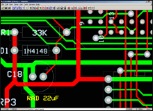
Place components and route traces on any grid size. Generate copper pours just the way you want them. Take advantage of CADint's integrated Specctra autorouter interface. And when it has all come together, generate your production files in a single step.

PCB layout features

  • Practically unlimited board size
  • Over 100 drawing layers including 32 copper layers, 16 mask layers, 14 hole type layers, 12 net-related layers, 11 documentation layers and more.
  • Support for through-hole, blind and buried vias.
  • Global resizing of padstacks across one, several or all symbols.
  • Pin, gate and component swapping.
  • Easily change footprints (through-hole, SMT, PLCC, etc) while maintaining netlist integrity.
  • Automatic renaming of component designators by topology, etc.
  • Powerful and flexible copper pour generation with:
     user definable clearances, outline width, line width, etc.
     thermal relief pad generation with user definable backoff and connection width.
     solid or cross-hatched pours with user definable line width, spacing and angle.
     automatic removal of unconnected and hanging areas.
  • On-line clearance check (defined by layer, category, and/or area on board) using definable manufacturing classes.
  • Electrical connectivity check of ratsnesting, unconnected parts.
  • Trace length, area, capacitance and line resistance calculations.
  • Crossprobing of components and nets.
  • 3D viewing of entire PCB or selected objects.
  • 3D clearance check of component packages.

Libraries

  • PCB symbol library with over 2500 footprints representing more than 10,000 components.
  • Flexible library structure supports generalized component types as well as specific part numbers.
  • Powerful library browser with preview, import, export, etc.
  • Graphical symbol and library editors.

Post-processing features

  • One-step generation of photoplotter and drill data to a zip file.
  • Powerful plotting module with:
     Flexible sheet set management for mixing various views on a single sheet.
     Output to any Windows printers.
     Output to file in graphics formats: DXF, Gerber, HPGL, Postscript and more.
     Print preview with full pan and zoom.
     Flexible title block and drawing annotation support.

  • Pick and Place output in MyData, Panasonic, SPEA or Siemens format.
  • Flexible Bill of Materials and Order List generation.
  • Test pads/netlist generation.
  • Design note functionality for annotation, drill table, board statistics and other documentation purposes.

Interfaces

  • Fully integrated transfer of layout to and from Specctra autorouter.
  • Import netlist from Cadence, EE Designer, Mentor Graphics, Protel, Tango or Vanguard.
  • Export netlist in EE Designer, EDIF 2 0 0, Tango or ThEDA format
  • Import PCB layout from CadStar, EDwin, EE Designer, IPL, Innoveda (PADS), P-Cad, Protel, Tango, Visula and more.
  • Export PCB layout in GenCAD or GenCAM format.
  • Import graphics in DXF or Gerber format.
  • Export graphics in Windows bitmap, DXF or Gerber format.

System features

  • Versatile graphics primitives, including:  line, arc, rectangle, circle, text, polygon  line and arc with definable thickness  filled circle  filled rectangle with definable corner radius
  • Display objects as centerline, outline or filled; in solid or transparent colors
  • Powerful properties/attributes handling
  • Rotate, copy, move, and/or mirror any group of objects
  • Automatic rubber-banding of wires, etc during move, stretch and/or rotate
  • 0.1 micron linear resolution
  • 0.001 degree angular resolution
  • Stepless pan and zoom
  • Context-sensitive (right-click) option menu available during any operation
  • Fully customizable accelerator keys and toolbar.

CADint PCB 3D-Viewer feature

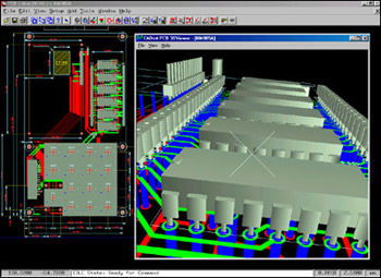
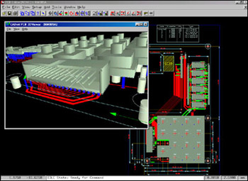
Use CADint's 3D Viewer to view your board at any magnification from any angle. View all or selected classes of board elements. Quickly and easily inspect complex routing, buried vias, clearance errors, etc. Take advantage of CADint's 3D package keepout polygons to visualize 3-dimensional component placement constraints.

The 3D viewer supports wireframe, solid and shadowed rendering with true or exaggerated z-scaling. Views may be exported as DXF files or copied to the Windows clipboard for insertion in reports, etc.

Contact

CADint Sweden AB
Enhagsslingan 3
187 40 Täby
Sweden
+46-8-4464133 | sales@cadint.se